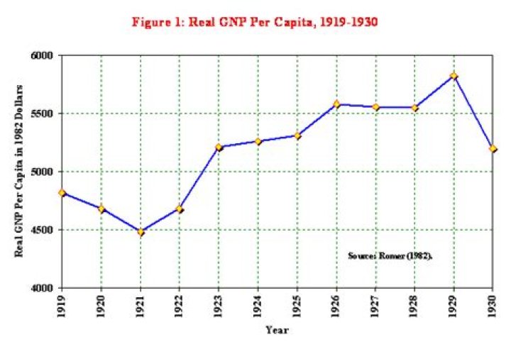
Lithography is the process of transferring patterns of geometric shapes in a mask to a thin layer of radiation-sensitive material (called resist) covering the surface of a semiconductor wafer. Figure 5.1 illustrates schematically the lithographic process employed in IC fabrication.
What is lithography technology?
A lithography system is essentially a projection system. Light is projected through a blueprint of the pattern that will be printed (known as a ‘mask’ or ‘reticle’). The blueprint is four times larger than the intended pattern on the chip.
What do you mean by photolithography?
Photolithography, also called optical lithography or UV lithography, is a process used in microfabrication to pattern parts on a thin film or the bulk of a substrate (also called a wafer).
What is lithography semiconductor?
A semiconductor lithography system undertakes a process whereby highly complex circuit patterns drawn on a photomask made of a large glass plate are reduced using ultra-high-performance lenses and exposed onto a silicon substrate known as a wafer. …
What is lithography and types?
Lithography, which is also called optical lithography or UV lithography, is a process used in microfabrication to pattern parts of a thin film or the bulk of a substrate. It uses light to transfer a geometric pattern from a photomask to a light-sensitive chemical “photoresist”, or simply “resist,” on the substrate.
What is lithography in science?
Lithography is the process of transferring a pattern onto a surface. In optical lithography, a physical mask covers a light sensitive film as it is exposed to (usually ultraviolet) radiation. Electron lithography instead draws the pattern by scanning a beam of electrons. A solution then develops the exposed film.
What is lithography equipment?
Lithography equipment transfers circuit or device patterns onto a substrate using a patterned mask and a beam of light or electrons to selectively expose a photo resist layer. Overlay metrology systems align the pattern masks or reticles.
What are the different types of lithography?
Overview. There are different types of lithographic methods, depending on the radiation used for exposure: optical lithography (photolithography), electron beam lithography, x-ray lithography and ion beam lithography.
What is photolithography in electronic devices?
Photolithography is the standard method of printed circuit board (PCB) and microprocessor fabrication. The process uses light to make the conductive paths of a PCB layer and the paths and electronic components in the silicon wafer of microprocessors. This process hardens a photo-resistive layer on the PCB or wafer.
What is photolithography with example?
1 : lithography in which photographically prepared plates are used. 2 : a process involving the photographic transfer of a pattern to a surface for etching (as in producing an integrated circuit) Other Words from photolithography Example Sentences Learn More About photolithography.
What is a lithography used for in semiconductor manufacturing?
Photolithography is a process used in microfabrication to transfer geometric patterns to a film or substrate. Geometric shapes and patterns on a semiconductor make up the complex structures that allow the dopants, electrical properties and wires to complete a circuit and fulfill a technological purpose.
What are the steps of lithography?
A step-by-step guide to stone lithography
- Graining the stone. Once a stone has been printed from for the last time, it is necessary to re-grain the stone to remove the greasy image and enable the stone to be re-used.
- Drawing on the stone.
- Processing the stone.
- Washing out and rolling up.
- Printing the stone.
What is the difference between photolithography and optical lithography?
For the same process applied to metal, see photochemical machining. Photolithography, also called optical lithography or UV lithography, is a process used in microfabrication to pattern parts on a thin film or the bulk of a substrate (also called a wafer).
What is the difference between photolithography and directed self assembly?
Photolithography is the standard method of printed circuit board (PCB) and microprocessor fabrication. Directed self-assembly is being evaluated as an alternative to photolithography. The root words photo, litho, and graphy all have Greek origins, with the meanings ‘light’, ‘stone’ and ‘writing’ respectively.
What is the importance of photolithography in semiconductor industry?
Photolithography would later contribute to the development of the first semiconductor ICs as well as the first microchips. Simplified illustration of dry etching using positive photoresist during a photolithography process in semiconductor microfabrication (not to scale).
Is excimer laser lithography the future of semiconductor manufacturing?
With the rapid advances made in tool technology in the last two decades, it is the semiconductor industry view that excimer laser lithography has been a crucial factor in the continued advance of Moore’s Law, enabling minimum features sizes in chip manufacturing to shrink from 800 nanometers in 1990 to 7 nanometers in 2018.